

Imaging From A to D, Part 1: From Photons to Voltages to Bits
Often taken for granted, analog to digital conversion is a crucial step in imaging
In the last few years, CMOS image sensors have displaced CCDs from the majority of consumer and industrial image capture applications. The success of CMOS has been driven in part by its potential to allow more functionality on the chip than was practical with CCDs. Many functions that used to require separate chips have moved on to the imaging sensor: analog to digital conversion (aka A to D, ADC or A/D), power conditioning, timing control, internal clock drivers, and a host of output interface options, from serializers to various parallel protocols. This has allowed lower power consumption, higher speeds, and smaller systems…but required extensive and intensive development in circuit design. Ultimately, CMOS imagers can also integrate signal processing and actual image processing to become “smart” sensors, but the complexity required takes them outside today’s mainstream.
ADC is a critical function for an imaging system. To understand why, it’s necessary to understand how CCDs and CMOS imagers work. Modern computing is overwhelmingly digital, so much so that old-school analog and mixed-signal circuit design sometimes seems like a black art. But it is crucial; to get an image into a computer for manipulation, you must convert analog signals to digital bits. Film is another analog medium…you can’t Photoshop a paper photo without scanning (digitizing) it, and the same is true for an analog video signal. There are no internet cat photos without ADC.
CCD vs. CMOS and Why ADCs Work
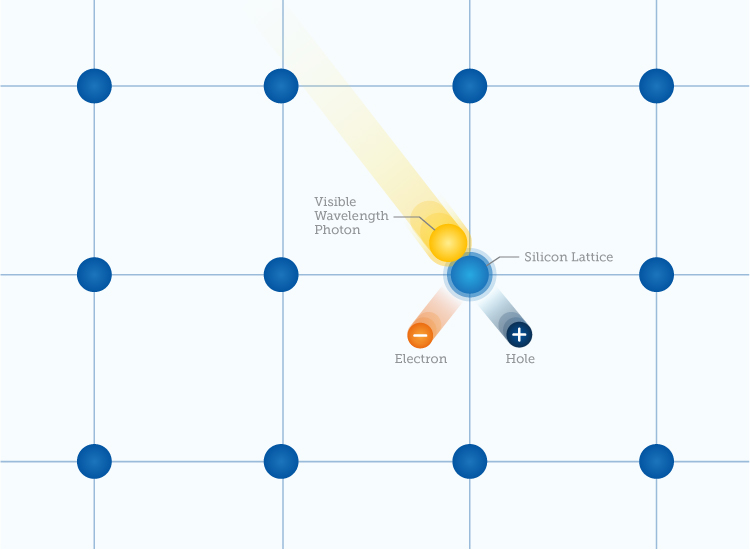
Both CCD and CMOS imagers collect charge in their silicon pixels by the photoelectric effect. To find out how much charge is in each pixel, it must be measured. This is done with a capacitor, which produces a voltage proportional to the charge. This voltage can then be amplified and sent off-chip to the outside world. In CCDs the charge to voltage conversions and amplification happens sequentially at one output node (or sometimes several) before it leaves the chip, one pixel at a time.
To get decent throughput, CCD output amplifiers must operate blazingly fast, because all the pixels of the entire array are waiting for them (think one checkout open at the grocery store)—this means speed limits and high power consumption (among other things). In contrast, modern CMOS pixels each do their own charge to voltage conversion and amplification in parallel. This means they can operate with lower power because each conversion can be slower (many hands make light work). In both CCD and CMOS, at this point the pixel signals are still analog.
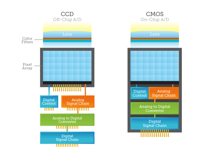
With CCDs, you must feed the chip’s analog output to an external ADC. The first CMOS imagers were also analog output, but the advance of circuit design and fabrication technology makes it possible and in many cases advantageous to integrate ADC on-chip. Why? It makes the complete system smaller and more convenient (although the chip itself is more complex to design).
The number of on-chip ADCs varies according to the purpose of the chip, but high-speed CMOS imagers now often use an ADC for each column of the pixel array (e.g. a 4k imager with 4096 ADCs). Massive parallelism again allows designers to crank up the total throughput even if each ADC is relatively modest in performance–imagine 4000+ grocery checkout lanes. It is also possible to put an ADC in every pixel, allowing digital pixel output—the ultimate in integration. The problem with this approach is that the ADC circuits take up space, and putting them in every pixel makes for big pixels that have very little space left to do actual light collection. Stacked architectures, with transistors layered under the photosensitive surface of the pixels, are now providing new possibilities, but the sweet spot for high-speed machine vision at present is column ADCs.
Since it is one of the limiters in the processing chain, optimizing ADC is crucial to overall imaging performance. In addition to throughput restrictions, the level of precision (number of bits) an ADC can produce can limit image quality, but adding more precision also slows down the conversion. The very act of conversion can also introduce noise to a signal, further reducing fidelity and image quality. And since ADCs require space and consume power, they affect chip size and therefore cost.
So how exactly do ACDs work? Stay tuned for the next installment of this series.