

Imaging From A to D, Part II: Design Priorities and Challenges
Often taken for granted, analog to digital conversion is a crucial step in imaging
Part 1 of this series reviewed how solid state imagers turn photons into voltages, and why those voltages need to become bits. In this installment, we look more closely at how ADCs accomplish that task.
ADCs convert continuous physical quantities to representative but discrete digital numbers. How does that work? Teledyne DALSA has a mixed signal CMOS design group that focuses on innovative, leading edge mixed signal circuit design for a variety of applications, including imaging but also audio. We asked Clemens Mensink, Ph.D., Business Development Manager, and Ed Van Tuijl, Ph.D., Principal Scientist, to dispense some of their wisdom on ADCs and what matters in their design.
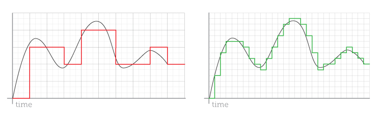
Machines that do continuous-to-discrete conversion go back to antiquity—ancient engineers in both Greece and China built geared clocks powered by flows of water. In today’s electronic ADCs, the output is a string of bits; represented visually, the smooth curves of analog signals become disconnected dots or chunky bar charts in the digital domain, no longer continuous in amplitude or time. But sampled often enough (with sufficient frequency, according to the famous Nyquist-Shannon theorem), in the right way, digital values contain all the information of the analog signals and can even be interpolated back to faithful reproductions of the original. “Can” is the important caveat here—perfect reproduction is rare. There are audiophiles who still cling to vacuum-tube-based analog high-fidelity equipment and argue that digital formats such as low bit rate MP3 figuratively turns fine wine into vinegar.
Not all ADCs are created equal. There are different ways to accomplish the task. Different approaches bring different strengths and weaknesses, and lend themselves to the optimization of different applications. With ADCs, as with any circuit, designers face many tradeoffs.
Speed is always a concern, since high frequency sampling means more accuracy, but speed often comes at the cost of higher power and noise. High resolution machine vision cameras delivering hundreds of frames per second have tremendous demands in terms of speed.
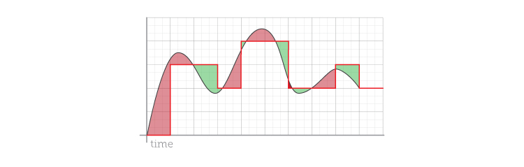
In trying to quantify an accurate digital representation of a continuous analog signal, digitizers must truncate or round values to the closest digital value, thus introducing quantization error. Accuracy also depends on the linearity of the converter—if for example it converts 1 volt into a digital number value of 25, will it convert 2 volts into 50, 3 volts into 75, and 4 volts into 100? Since ADCs are physical objects, they are subject to imperfections; perhaps 2 volts becomes 49 while 3 volts becomes only 72—or 60 or 87. If nonlinear behavior is known (by calibration) it can be corrected, but unpredictable nonlinearity reduces accuracy—stable, repeatable performance is paramount to a system designer.
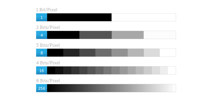
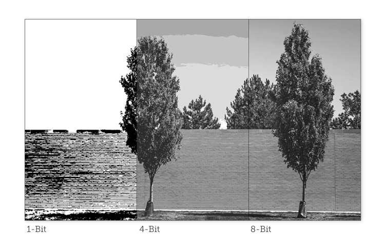
Circuit designers must also balance the level of precision their ADCs provide. In image quality terms, more bit depth allows (but does not guarantee) more levels of detail. Eight bits (256 distinct levels) is common in imaging, but some applications require even finer gradations. Scientific imaging often needs 12 bits (4096 levels). Medical imaging such as x-ray looks for 14 or 16 bits (65536 levels). High-end audio applications stretch beyond 20 bits. The tradeoffs in providing high bit depth/precision depend on the approach, but can include speed limitations, chip complexity and space requirements.
It should be noted that having 8 or 12 or 16 possible bits of precision does not guarantee that a design can actually deliver that many levels. In practice, all real ADCs have some level of noise and distortion, reducing the practical precision and accuracy. Random noise is the enemy of precision. If your system has 12-bit ADCs (4096 levels) but also produces random noise that cause a variance of four levels (+/- 2), you cannot trust your system to accurately report differences of one level in 4096. The best you can do in that situation is 4/4096 or one in 1024 levels, which is only ten bits (1024 =2^10). You lose two bits of precision to noise. Noise from any and all sources must be minimized at every turn.
All designs must pay attention to power—high power dissipation means heat and noise, and it limits not only performance but the type of applications that can be served. High power designs place more demands on the overall system (including more size more cost) and, as every owner of a cell phone can attest, are ill-suited to small and mobile applications.
The amount of space an ADC circuit takes on a chip is another important consideration. In the parallel ADCs of machine vision imagers, the ADCs circuits might only be one pixel wide, and with high resolution sensors that use small pixels (2-5 µm), this can be a significant restriction. In other designs, such as X-ray detectors, size is far less of an issue–the pixels are often over 100 µm wide, and ADCs could be placed inside the pixels themselves. Stacked architectures offer new possibilities for maximizing pixel area, but they bring their own challenges in design and fabrication. In audio ADCs, there are no pixels at all, but circuit size is still important, since increasing the size of a chip reduces the number that will fit on a silicon wafer. The cost of fabricating a wafer is the same whether it has one device or 1000 devices on it, so the smaller the device, the lower the cost of each individual chip.
Calibration is an often overlooked aspect of ADC design. Some designs require initial and periodic active calibration to provide good results. This means a delay every time the end user presses the “On” switch, as well as interruptions in operation later, to say nothing of increased power and space requirements. At best this is inconvenient; at worst it rules out that design for many applications. It requires creativity and innovation to deliver circuits that calibrate “by design”—for example, by careful passive component choice instead of by running active routines based on stored data–but the end result is a smaller, faster, better system.
Given all these competing goals, what are the actual designs used in the machine vision industry and how do they work? Stay tuned for Part III.
 Imaging From A to D, Part 1: From Photons to Voltages to Bits
  “In engineering, there is always something to massage”